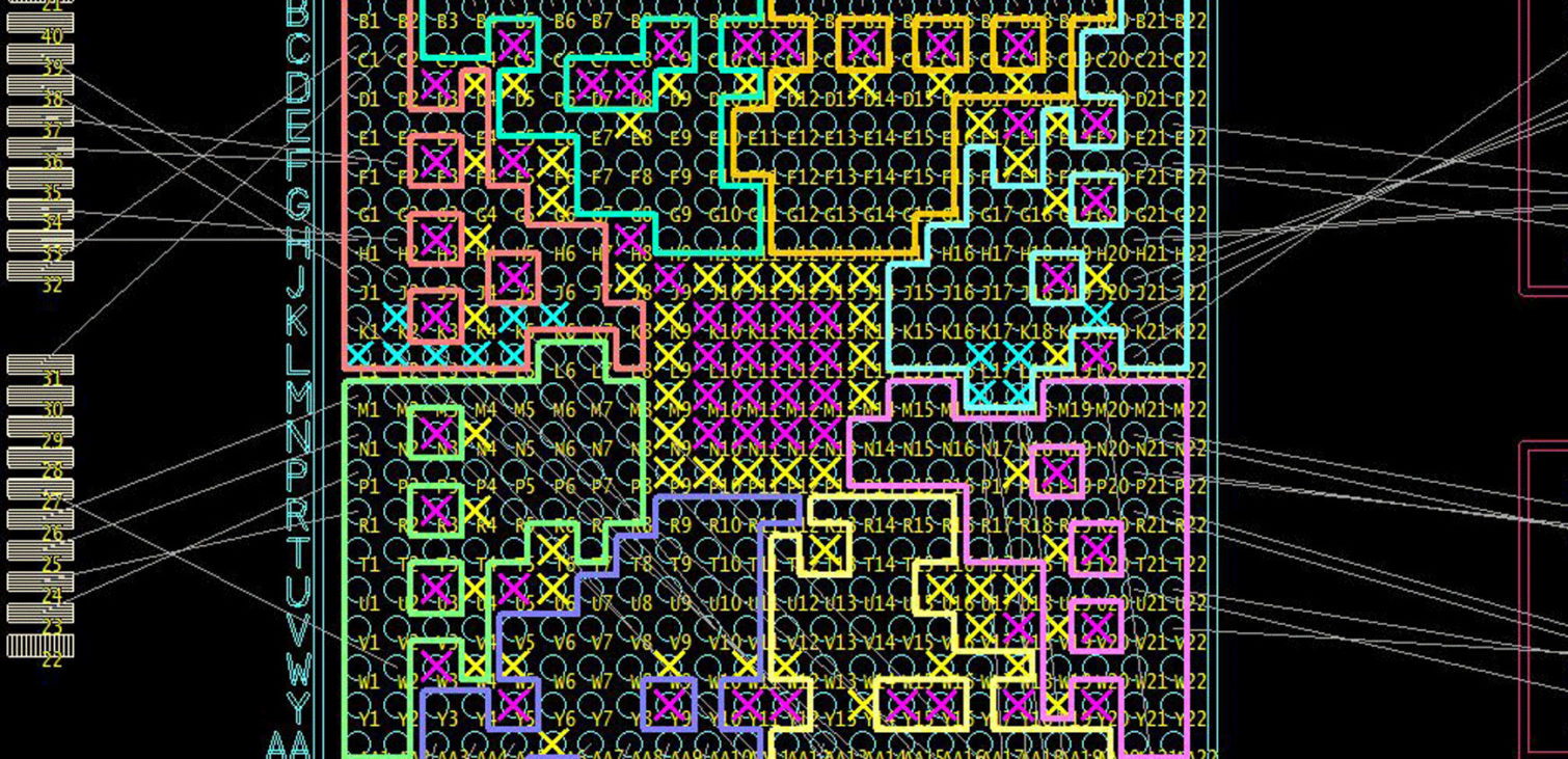
FPGA Design
RTL design in VHDL and SystemVerilog for Xilinx, Intel, and Lattice silicon — signal processing, custom interfaces, and SoC integration.
Most of our FPGA work involves either greenfield designs or extensions to existing IP. We handle the full flow — RTL, simulation, synthesis, place-and-route, and bring-up — and we use UVM testbenches and CI for verification.
Get in TouchCapabilities
The work that comes up on most FPGA projects.
RTL Design
VHDL and SystemVerilog. Pipelined data paths, clock-domain handling, and resource-aware coding.
Verification
UVM testbenches with constrained-random stimulus and functional coverage. Formal methods where they fit.
Timing Closure
Static timing analysis, retiming, pipelining, and SDC constraints to meet target frequency.
DSP & Signal Processing
FIR/IIR filters, FFTs, mixers, decimators, and DDC chains. Fixed-point arithmetic verified against a model.
High-Speed Interfaces
PCIe, multi-gigabit Ethernet, JESD204, MIPI CSI/DSI, DDR memory controllers, and custom SERDES protocols.
SoC Integration
Zynq, Versal, and Intel SoC FPGAs. Linux on the PS side, custom IP on the PL side, and AXI plumbing between.
Tools & silicon
The vendor toolchains, simulators, and silicon families we work with regularly.
Common use cases
Camera Pipelines
MIPI CSI-2 ingestion, image processing, and pre-processing for AI accelerators on Zynq and Versal SoCs.
High-Speed Data Acquisition
ADC interfacing over JESD204, real-time DSP, and PCIe DMA for instrumentation and software-defined radio.
Motor Control
Field-oriented control, encoder feedback, current loops, and EtherCAT slaves implemented in the FPGA fabric.
Protocol Bridges
Translating between legacy industrial buses, Ethernet, and proprietary backplane protocols.
Have an FPGA project?
Tell us about it. We'll review and reply within one business day.